


SEMICONDUCTOR
Laser processing solutions for semiconductor
Laser technology is widely applied into the semiconductor industry, such as online/ offline PCB marking and PCBA cutting, flexible PCB marking and PCBA cutting, full-automatic IC marking and so on.
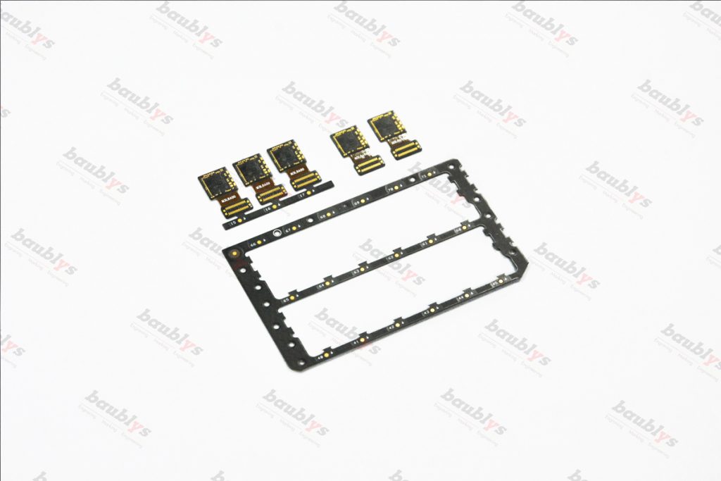
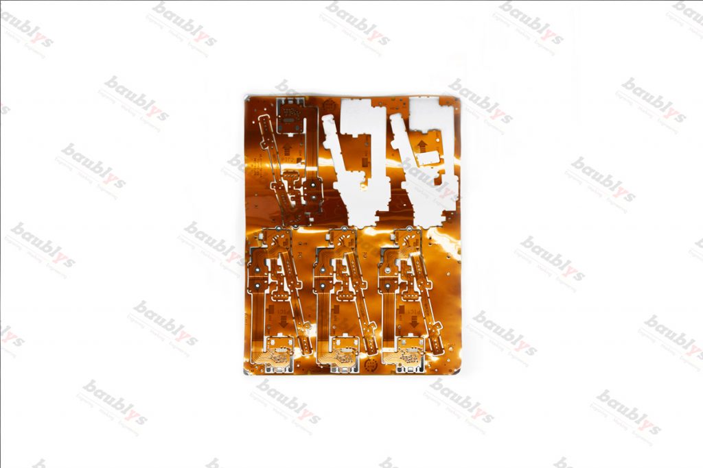
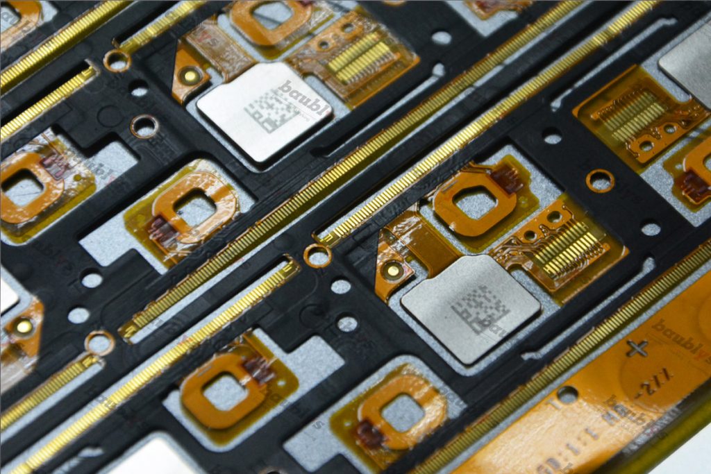
Semiconductors and small electronic components are usually produced in very large quantities. Economic mass production is only possible through fully automated processes. The small components often have to be provided with much information. This information must be flexibly and extremely quickly applied to the components.
By using a laser system with a galvo head for very fast deflection of the laser beam and a partially or fully automated solution, the high requirements can be met. The applied marking is resistant, durable and perfectly readable.
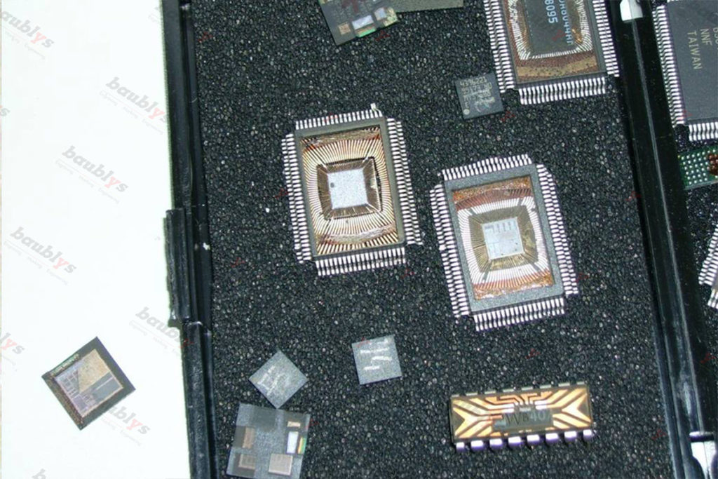
A laser system is also used for special test procedures of microchip testing, also called decapping.
Decapping a microchip into a process of removing the protective coating of a microchip so that the actual chip itself is revealed for visual inspection of the microcircuits. This process is typically performed to debug a manufacturing problem with the chip or possibly copy information from the chip.
Possible laser marking methods:
- Annealing
- Marking and cutting foils
- Colored annealing
- Color / anodizing and paint removal
- Surface structuring
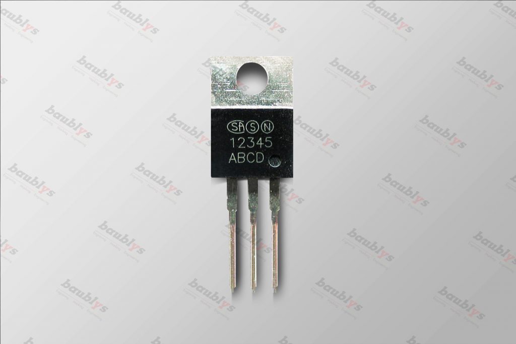
- Marking
- Deep engraving
- 3D deep engraving
- Laser cutting
- Foaming
- Carbonization
Some other application examples
More applications on semiconductor industry
-
- Decapping of microchips
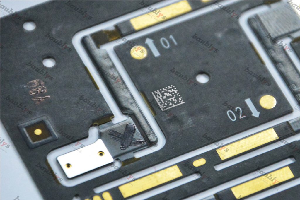
- Marking information and logos
- Marking consecutive serial numbers
- Cutting materials
- Marking of raw materials and finished products
- Marking of 1D & 2D codes
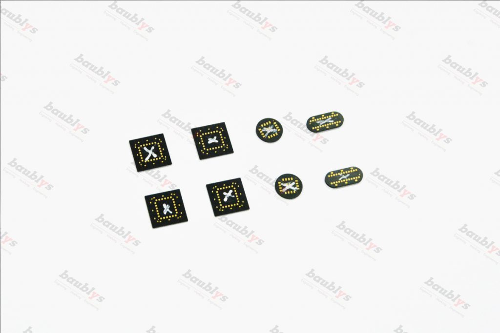
- Marking of semiconductors and other electronic components / assemblies / SMD
Advantages
High efficiency is achieved by an extremely flexible laser marking system, which adapts quickly to changing requirements.
High economic efficiency, identification, traceability, quality assurance through testing with integrated camera, database connection with feedback of the labeling, high quality, durable and permanent marking, optimal and long-lasting readability.